TE Connectivity PCB 2.8 Montage
Inhaltsverzeichnis
Quicklinks
NOTE
THE BOUNDARY CONDITIONS IN THIS SPECIFICATION HAVE NOT BEEN TESTED ON THE TERMINAL.
IN CASE OF INCOMPLETENESS AND FOR CHANGE REQUESTS CONTACT THE RESPONSIBLE TYCO
ELECTRONICS ENGINEERING GROUP.
IN CASE OF CONFLICT GERMAN TEXT IS BENDING
ANMERKUNG
DIE RANDBEDINGUNGEN IN DIESER SPEZIFIKATION WURDEN NICHT AN DEN KONTAKTEN
GEPRÜFT. ÄNDERUNGEN WERDEN VORBEHALTEN.
UNVOLLSTÄNDIGKEITEN UND ÄNDERUNGSWÜNSCHE SIND AN TYCO ELECTRONICS ZU MELDEN.
IM ZWEIFEL GILT DER DEUTSCHE TEXT.
Table of Contents
1
2
2.1
2.2
3
3.1
3.2
4
4.1
4.2
4.2.1
4.2.2
4.3
Soldering
4.4
Assembly Instructions
4.4.1
Assembly with fuse and relais
5
GENERAL NOTE
Tyco Electronics Corporation,
Harrisburg, PA 17105
*
Trademark
| Indicates change
Application Specification
Verarbeitungs-Spezifikation
PCB 2.8 PCB 6.3 PCB 9.5
2
2
2
2
2
2
3
3
3
6
6
6
8
10
10
11
Product Information Center +49 (0) 6251 1999
Inhaltsverzeichnis
1
ANWENDUNGSBEREICH
2
ZUSÄTZLICHE UNTERLAGEN
2.1
Kundenzeichnung
2.2
Produktspezifikation
3
BESCHREIBUNG
3.1
Varianten
3.2
Funktionen
4
VERARBEITUNG
4.1
Max. zugelassene Kräfte
4.2
Montage
4.2.1
4.2.2
4.3
4.4
4.4.1
5
ALLGEMEINERHINWEIS
This specification is a controlled document.
Copyright 2000 by Tyco Electronics Corporation.
All rights reserved
114-18910
10. Nov. 2015
Rev. D
2
2
2
2
2
2
3
3
3
6
6
6
8
10
10
11
1 of 11
ECOC EGA0
LOC: AI
Inhaltsverzeichnis

Verwandte Anleitungen für TE Connectivity PCB 2.8


Inhaltszusammenfassung für TE Connectivity PCB 2.8
-
Seite 1: Inhaltsverzeichnis
Application Specification 10. Nov. 2015 Rev. D Verarbeitungs-Spezifikation PCB 2.8 PCB 6.3 PCB 9.5 NOTE THE BOUNDARY CONDITIONS IN THIS SPECIFICATION HAVE NOT BEEN TESTED ON THE TERMINAL. IN CASE OF INCOMPLETENESS AND FOR CHANGE REQUESTS CONTACT THE RESPONSIBLE TYCO ELECTRONICS ENGINEERING GROUP. -
Seite 2: Scope
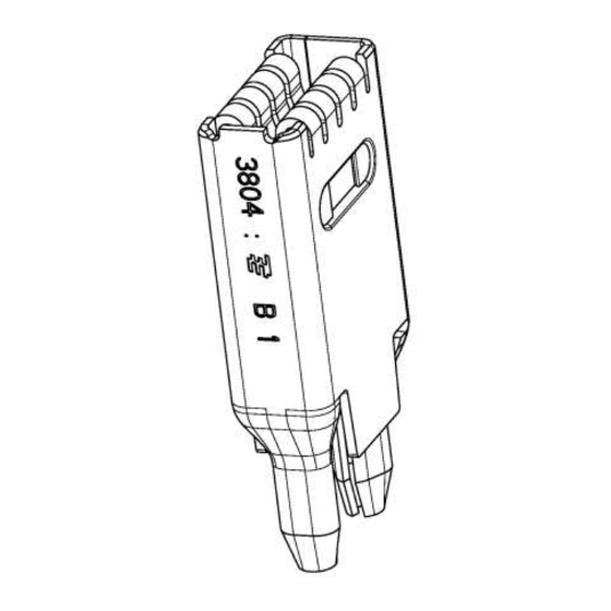
114-18910 SCOPE ANWENDUNGSBEREICH This specification covers processing Diese Spezifikation beinhaltet die Richtlinien zur requirements of the PCB terminal. Verarbeitung der PCB-Kontakte. ADDITIONAL DOCUMENTS ZUSÄTZLICHE UNTERLAGEN Customer Drawing Kundenzeichnung There is a customer drawing for each part number, Für jede Bestell-Nr. gibt es eine Kundenzeichnung showing the dimensions and materials of the mit den Maßen und Werkstoffen des Kontaktes. -
Seite 3: Functions
114-18910 Functions Funktionen The terminal provides following functions necessary Kontakt verfügt über folgende für for application (see Figure 4): Verarbeitung notwendige Funktionen (siehe Bild 4): - Mating area to the contact zone - Einführungsbereich zur Kontaktzone - Connection to carrier strip - Anbindung für Trägerstreifen - Contact protection - Kontaktschutz... - Seite 4 114-18910 Figure 4 / Bild 4 functional areas / Funktionsbereiche Figure No. Description Force Direction ± 5° MAX. Force [N] ± 10% Detail of position Bild Nr. Beschreibung Kraftrichtung ± 5° Max. Kraft [N] ± 10% Detail der Position contact lamella Kontaktlamelle Solder pin Locking side...
- Seite 5 114-18910 Figure 5 / Bild 5 Figure 6 / Bild 6 Figure 7 / Bild 7 Force contact lamella Force solder pin Force side wall Kraft Kontaktlamelle Kraft Lötpfosten Kraft Seitenfläche Figure 8 / Bild 8 Figure 9 / Bild 9 Force contact protection force mating side Kraft Kontaktschutz...
-
Seite 6: Assembly
114-18910 Assembly Montage 4.2.1 Assembly with carrier strip 4.2.1 Montage mit Trägerstreifen Preferably, the contact is processed as strip-ware. Vorzugsweise wird der Kontakt als Bandware verarbeitet. Bei der Verarbeitung von Bandware mit During the processing of strip-ware on PCB by a einem geeigneten Automaten wird größtmögliche suitable automat the highest quality is achieved. - Seite 7 114-18910 1719103 1719102 1719101 Figure 10 / Bild 10 Layout / mögliches Layout Figure 11 / Bild 11 Figure 12 / Bild 12 Flächen zum Einpressen / Einpresswerkzeug Einpresswerkzeug / Surface for force fitting Application tool Figure 13 / Bild 13 Eingebaut in Handpresse / Application tool installed at hand lever press Rev.
-
Seite 8: Lötung
114-18910 Soldering Lötung The terminal is soldered on the PCB, there are a Der Kontakt wird auf der Leiterplatte verlötet. Hier proved wave-soldering maschine with nitrogen haben sich Wellenlötanlagen mit Stickstoffum- environment. gebung bewährt. Eine bewährte Lötkurve wird in A proven solder curve is shown in Figure 14. This Bild 14 gezeigt. - Seite 9 114-18910 Figure 14 / Bild 14 soldering diagramm and measuring points / Lötkurve und Messpunkte Rev. B 9 of 11...
-
Seite 10: Hinweise Bestückung
114-18910 Assembly Instructions Hinweise Bestückung 4.4.1 Assembly with fuse and relais 4.4.1 Bestückung mit Sicherung und Relais Usually the terminal is applied with a fuse or a relay. Der Kontakt wird üblicherweise mit einer Sicherung Typical forces which may occur were determined by oder einem Relais bestückt. - Seite 11 R. MEIER 10NOV2015 SARAVANA BURGHARD, GENERAL NOTE ADDED 08NOV2017 KUMAR.M MICHAEL SANDEEP KHADRI TE Connectivity Germany GmbH 02.03.2014 Ampèrestraße 12-14 64625 Bensheim A. LEHNER H. ULRICH 114-18910 PCB CONTACT 2.8; 6.3; 9.5 MM VERARBEITUNGS-SPEZIFIKATION TITLE PCB CONTACT 2.8; 6.3; 9.5 MM APPLICATION SPECIFICATION Rev.